The importance of light-based technologies for our society was demonstrated once more in recent weeks. Thanks to the internet, millions of people can work remotely, enter virtual classrooms, or talk to friends and relatives. The internet, in turn, owes its power to countless light pulses with which enormous amounts of data are sent around the globe via optical fibres.
To steer and control these light pulses, various technologies are employed. One of the oldest and most important is the diffraction grating, which deflects light of different colours in precisely determined directions. For decades, scientists have been trying to improve the design and production of diffraction gratings to make them suitable for today’s demanding applications. At ETH Zurich, a group of researchers led by David Norris, professor at the Department of Mechanical and Process Engineering, have developed a completely new method by which more efficient and more precise diffraction gratings can be produced. They did this together with colleagues now at the University of Utrecht and the company Heidelberg Instruments Nano, which was founded as ETH spin-off SwissLitho. The researchers published the results in the scientific journal Nature.
Interference through grooves
Diffraction gratings are based on the principle of interference. When a light wave hits a grooved surface, it is divided into many smaller waves, each emanating from an individual groove. When these waves leave the surface, they can either add together or cancel each other, depending on the direction in which they travel and on their wavelength (which is related to their colour). This explains why the surface of a CD, on which data is stored in tiny grooves, generates a rainbow of reflected colours when it is illuminated by white light.
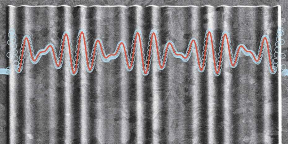
For a diffraction grating to work properly its grooves need to have a separation similar to the wavelength of the light, which is around one micrometre – a hundred times smaller than the width of a human hair. “Traditionally, those grooves are etched into the surface of a material using manufacturing techniques from the microelectronics industry”, says Nolan Lassaline, a PhD student in Norris’s group and first author of the study. “This means, however, that the grooves of the grating are rather square in shape. On the other hand, physics tells us that we should have grooves with a smooth and wavy pattern, like ripples on a lake.” Grooves made with traditional methods can, therefore, only ever be rough approximations, which in turn means that the diffraction grating will steer light less efficiently. By pursuing a completely new approach Norris and his collaborators have now discovered a solution to that problem.
Surface patterning with a hot probe
Their approach is based on a technology that also has its origins in Zurich. “Our method is a great-grandchild of the scanning tunnelling microscope, which was invented almost forty years ago by Gerd Binnig and Heinrich Rohrer, who would later win the Nobel Prize for their work”, says Norris. In such a microscope, material surfaces are scanned by the sharp tip of a probe with high resolution. The images resulting from such a scan can even show the individual atoms of a material.
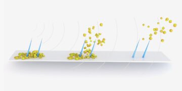
Conversely, however, one can also use the sharp tip to pattern a material and thus produce wavy surfaces (see picture). To do so, the researchers heat the tip of a scanning probe to almost 1000 degrees centigrade and press it into a polymer surface at certain locations. This causes the molecules of the polymer to break up and evaporate at those locations, allowing the surface to be precisely sculpted. In this way, the scientists can write almost arbitrary surface profiles point by point into the polymer layer with a resolution of a few nanometres. Finally, the pattern is transferred to an optical material by depositing a silver layer onto the polymer. The silver layer can then be detached from the polymer and used as a reflective diffraction grating.
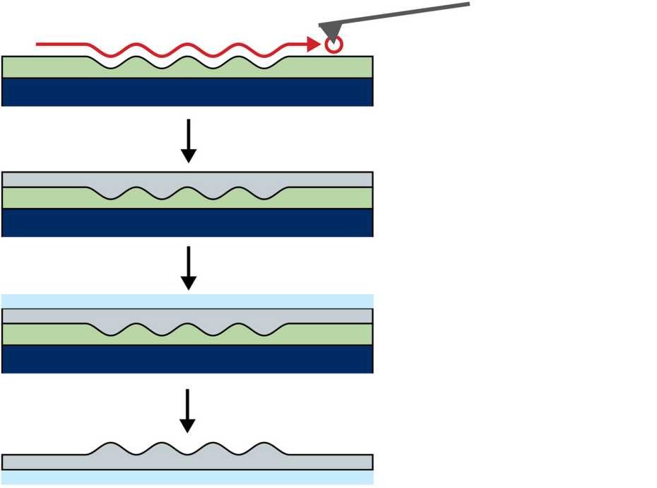
At ETH diffraction gratings are produced by patterning a polymer layer (green) with a hot scanning probe. A silver layer (grey) is then deposited, which is finally detached with a glass slide (blue). (Visualisations: ETH Zurich / Nolan Lassaline)

This allows us to produce arbitrarily shaped diffraction gratings with a precision of just a few atomic distances in the silver layer”, says Norris. Unlike traditional square-shaped grooves, such gratings are no longer approximations, but practically perfect and can be shaped in such a way that the interference of the reflected light waves create precisely controllable patterns.
A variety of applications
Such perfect gratings enable new possibilities for controlling light, which has a range of applications, says Norris: “The new technology can be used, for instance, to build tiny diffraction gratings into integrated circuits with which optical signals for the internet can be sent, received and routed more efficiently.” Lassaline adds, “Generally, we can use such diffraction gratings to make highly miniaturized optical devices such as on-chip micro-lasers.” Those miniaturized devices, he says, range from ultrathin camera lenses to compact holograms with sharper images. They promise a broad impact in optical technologies such as futuristic smartphone cameras, biosensors, or autonomous vision for robots and self-driving cars.


