In recent years, 2-dimensional (2D) Cheap and energy-efficient electronics materials such as graphene are making waves in scientific world due to their unique physical, chemical, and electronic properties and high potential applicability in flexible electronics, strain sensors, nanogenerators, innovative nanoelectromechanical systems (NEMS) and so on. Graphene is not the only candidate of a whole family of 2D materials. Now we have 2.5D materials (Emergence of 2.5D Materials for Futuristic Applications) that are likely to have huge impact on futuristic applications.

The other cousins such as MXenes, oxides, boron nitride, transition metal chalcogenides, metal-organic frameworks, clays, polymers also belong to the same family of 2D materials. 2D materials, like graphene, are made of a single layer of atoms and are used in applications for next generation flexible electronic evolution, including electromechanical sensors, biomedical devices, energy storage, field effect transistors, supercapacitors and so on.
The next generation materials, so called 2.5D materials offers a novel approach to synthesizing materials with unique properties by controlling their weak out-of-plane van der Waals (vdW) interactions. Researchers from Global Innovation Center, Kyushu University, Fukuoka and other universities from Japan are intensively pursuing research to find new strategies to artificially stack two-dimensional (2D) materials, introducing 2.5D materials with unique physical properties. These researchers have reviewed the latest advances and applications of 2.5D materials in the journal Science and Technology of Advanced Materials(Science of 2.5 dimensional materials: paradigm shift of materials science toward future social innovation).
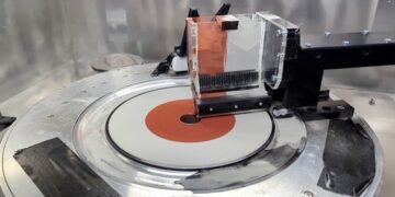
In a new concept,different 2D materials are artificially stacked together either in a vertical plane or at twisted angles by using advanced transfer technique (1,2), irrespective of their, lattice constants or composition. This is feasible because our ability to control weak plane van der Waals (vdW) electrical interactions between atoms and molecules and since the stacks are not limited by rigid chemical bonds. In addition, there is a possibility to integrate 2D materials with other dimensional materials – molecules and ions (zero-dimensional (0D)), nanotubes and nanowires (one-dimensional (1D)), and bulk crystals (three-dimensional (3D)).
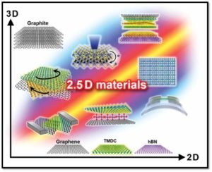
As illustrated in Figure 1, there is a symbiotic relationship between bulk 3D materials and 2D materials. We call these new materials and architectures ‘2.5D materials,’ where the 0.5D signifies the new dimension created by combining 2D materials through artificial manipulations, such as stacking, twisting, and connecting as well as through the 2D nano- space within 2D material stacks.
There is an exciting possibility that these next generation 2D materials will make enormous impact on diverse fields, including Internet of Things, Artificial Intelligence, Quantum Computing, energy production/storage/efficiency, blockchain, drones, 3D printing and virtual reality (VR) so on.
2.5D materials – four important research topics:
- Material synthesis: The growth and transfer (by specialized robotic transfer techniques) of individual 2D materials are key processes for the fabrication of 2.5D materials. Among the various growth methods, chemical vapor deposition (CVD) is widely used to prepare large-area single crystals of 2D materials as well as their polycrystalline films making new 2D materials as building blocks of various 2.5D materials. In addition, production of high-quality, large 2D material wafers, such as hBN sheets, is also important.Using the CVD method, the researchers selectively synthesized a bilayer of graphene, the simplest form of a 2.5D material, using copper-nickel foil with a relatively high nickel concentration as a catalyst. The nickel makes the carbon highly soluble, giving researchers more control over the number of graphene layers. When an electric field was applied vertically across the graphene bilayer, it opened a band gap, meaning its conductivity can be turned on and off. This is a phenomenon that is not observed in single-layer graphene because it has no band gap and stays on all the time. By tilting the stacking angle by one degree, the scientists discovered that the material became superconducting.
- van der Waals science: Both vertical stacking and in-plane connection of 2D materials. In the former, combining different types of 2D materials with controlled stacking angles is expected to offer new phenomena, such as moiré physics, to establish a new scientific field. As there are infinite combinations of materials, theories that can predict the physical properties of new 2.5D materials are needed.
- 2D nanospace: intercalation of molecules and ions to alter the physical properties of the host 2D materials, thus obtaining new ordered structures that could offer novel physical properties and phenomena. Moreover, 2D nanospace offers a unique reaction field for the growth of novel materials that cannot be obtained in usual environments.
- Applications: Solar cells, batteries, flexible devices, quantum devices, and devices with very low energy consumption are expected. In an. interesting example (4}. researchers have found that graphene stabilises iron chloride when it is inserted between its stacked layers, while inserting lithium ions leads to a faster diffusion rate (how quickly molecules spread in an area) than that of graphite, an electrical conductor used in batteries. This implies the material could be used in high-performance rechargeable batteries.
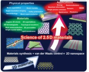
As shown in Figure 2, there are numerous possibilities to explore new materials science, and potentially have a strong impact on our future life. This new concept also requires strong collaborations between researchers working in different fields. Through such collaborative research on the basis of ‘2.5D materials,’ we believe that the new scientific field will be established which lead to a new era of materials science.
(Creative Commons CC )
Further Reading
- Pizzocchero F, Gammelgaard L, Jessen BS, et al. The hot pick-up technique for batch assembly of van der Waals heterostructures. Nat Commun. 2016; 7:11894.
- Masubuchi S, Morimoto M, Morikawa S, et al. Autonomous robotic searching and assembly of two-dimensional crystals to build van der Waals superlattices. Nat Commun. 2018; 9:1413
- A new age of 2.5D materials
- https://www.science20.com/news_staff/what_is_a_25d_material_and_will_it_make_future_tech_possible-256049
About Author
Dr. Yashwant R. Mahajan was Technical Advisor at International Advanced Research Centre for Powder Metallurgy and New Materials (ARCI), Hyderabad, and also at ARC-I’s Centre for Knowledge Management of Nanoscience and Technology (CKMNT), Hyderabad. He obtained his Ph.D. degree in Physical Metallurgy in 1978 from Polytechnic Institute of Brooklyn, New York. Dr. Mahajan made major contributions in the areas of MMCs, advanced ceramics, and CMCs. Under his leadership, a number of ceramic- based technologies were developed and transferred to the industry. He has published more than 130+ technical papers in peer-reviewed journals and conference proceedings and holds 13 patents (including 2 US). Dr. Mahajan is a recipient of NRC Associateship of National Academy of Sciences, USA, the best metallurgist of the year award (IIM), MRSI Medal, MRSI-IISC superconductivity award, and VASVIK Medal.


