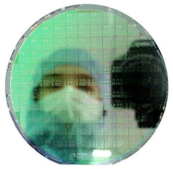
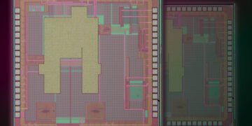
A wafer integrated with 2-D material. Credit: Arne Quellmalz, KTH Royal Institute of Technology
Experimental methods for transferring grown 2-D material to desired electronics have been beset by a number of deficiencies, such as degradation of the material and its electronic transport properties, or by contamination of the material.
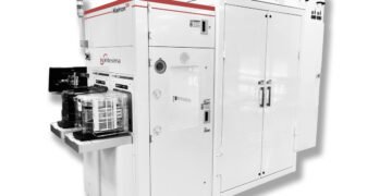
Quellmalz says that the solution lies in the existing toolkits of semiconductor manufacturing: to use a standard dielectric material called bisbenzocyclobutene (BCB), along with conventional wafer bonding equipment.
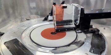
“We basically glue the two wafers together with a resin made of BCB,” he says. “We heat the resin, until it becomes viscous like honey, and press the 2-D material against it.”

A scalable method for the large-area integration of 2D materials.
Credit: Arne Quellmalz (Graphene Flagship/KTH Sweden).
At room temperature, the resin becomes solid and forms a stable connection between the 2-D material and the wafer, he says. “To stack materials, we repeat the steps of heating and pressing. The resin becomes viscous again and behaves like a cushion, or a waterbed, which supports the layer stack and adapts to the surface of the new 2-D material.”
The researchers demonstrated the transfer of graphene and molybdenum disulfide (MoS2), as a representative for transition metal dichalcogenides, and stacked graphene with hexagonal boron nitride (hBN) and MoS2 to heterostructures. All transferred layers and heterostructures were reportedly of high quality, that is, they featured uniform coverage over up to 100-millimeter sized silicon wafers and exhibited little strain in the transferred 2-D materials, the paper states.
