Scientists at the University of Bath have taken an important step towards understanding the interaction between layers of atomically thin materials arranged in stacks. They hope their research will speed up the discovery of new, artificial materials, leading to the design of electronic components that are far tinier and more efficient than anything known today.
Smaller is always better in the world of electronic circuitry, but there’s a limit to how far you can shrink a silicon component without it overheating and falling apart, and we’re close to reaching it. The researchers are investigating a group of atomically thin materials that can be assembled into stacks. The properties of any final material depend both on the choice of raw materials and on the angle at which one layer is arranged on top of another.
Dr. Marcin Mucha-Kruczynski who led the research from the Department of Physics, said: “We’ve found a way to determine how strongly atoms in different layers of a stack are coupled to each other, and we’ve demonstrated the application of our idea to a structure made of graphene layers.”
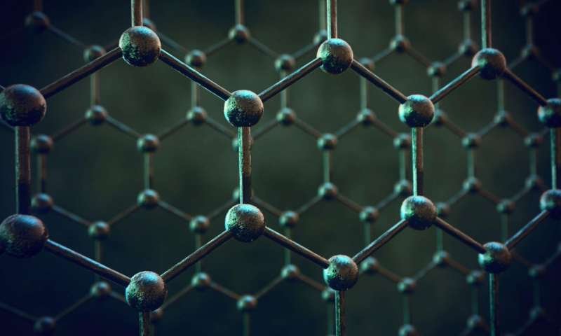
The Bath research, published in Nature Communications, is based on earlier work into graphene—a crystal characterized by thin sheets of carbon atoms arranged in a honeycomb design. In 2018, scientists at the Massachusetts Institute of Technology (MIT) found that when two layers of graphene are stacked and then twisted relative to each other by the ‘magic’ angle of 1.1°, they produce a material with superconductive properties. This was the first time scientists had created a super-conducting material made purely from carbon. However, these properties disappeared with the smallest change of angle between the two layers of graphene.
Since the MIT discovery, scientists around the world have been attempting to apply this ‘stacking and twisting’ phenomenon to other ultra-thin materials, placing together two or more atomically different structures in the hope of forming entirely new materials with special qualities.
“In nature, you can’t find materials where each atomic layer is different,” said Dr. Mucha-Kruczynski. “What’s more, two materials can normally only be put together in one specific fashion because chemical bonds need to form between layers. But for materials like graphene, only the chemical bonds between atoms on the same plane are strong. The forces between planes—known as van der Waals interactions—are weak, and this allows for layers of material to be twisted with respect to each other.”
The challenge for scientists now is to make the process of discovering new, layered materials as efficient as possible. By finding a formula that allows them to predict the outcome when two or more materials are stacked, they will be able to streamline their research enormously.
It is in this area that Dr. Mucha-Kruczynski and his collaborators at the University of Oxford, Peking University and ELETTRA Synchrotron in Italy expect to make a difference.
“The number of combinations of materials and the number of angles at which they can be twisted is too large to try out in the lab, so what we can predict is important,” said Dr. Mucha-Kruczynski.
The researchers have shown that the interaction between two layers can be determined by studying a three-layer structure where two layers are assembled as you might find in nature, while the third is twisted. They used angle-resolved photoemission spectroscopy—a process in which powerful light ejects electrons from the sample so that the energy and momentum from the electrons can be measured, thus providing insight into properties of the material—to determine how strongly two carbon atoms at a given distance from each other are coupled. They have also demonstrated that their result can be used to predict properties of other stacks made of the same layers, even if the twists between layers are different.
The list of known atomically thin materials like graphene is growing all the time. It already includes dozens of entries displaying a vast range of properties, from insulation to superconductivity, transparency to optical activity, brittleness to flexibility. The latest discovery provides a method for experimentally determining the interaction between layers of any of these materials. This is essential for predicting the properties of more complicated stacks and for the efficient design of new devices.
Dr. Mucha-Kruczynski believes it could be 10 years before new stacked and twisted materials find a practical, everyday application. “It took a decade for graphene to move from the laboratory to something useful in the usual sense, so with a hint of optimism, I expect a similar timeline to apply to new materials,” he said.
Building on the results of his latest study, Dr. Mucha-Kruczynski and his team are now focusing on twisted stacks made from layers of transition metal dichalcogenides (a large group of materials featuring two very different types of atoms—a metal and a chalcogen, such as sulphur). Some of these stacks have shown fascinating electronic behavior which the scientists are not yet able to explain.
“Because we’re dealing with two radically different materials, studying these stacks is complicated,” explained Dr. Mucha-Kruczynski. “However, we’re hopeful that in time we’ll be able to predict the properties of various stacks, and design new multifunctional materials.”


