This means they have remained bigger and slower than other technologies, like the silicon chip, that they integrate with.
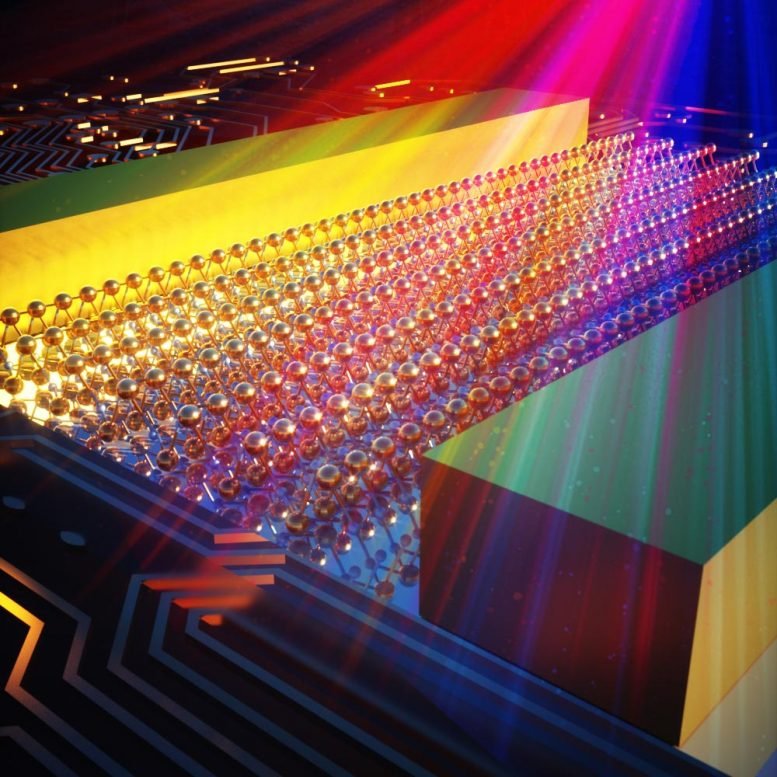
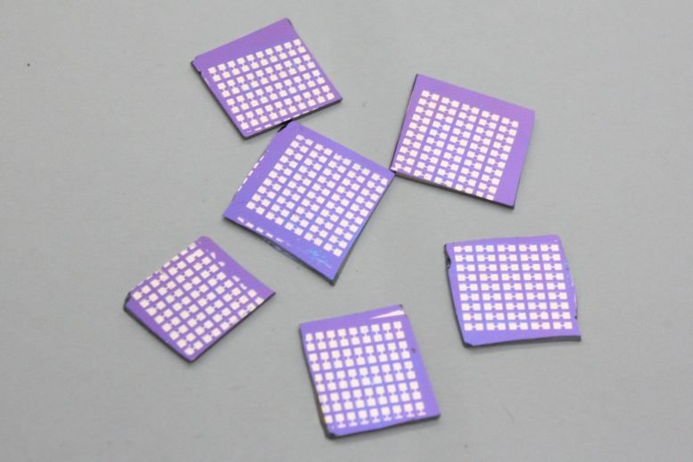
The new hyper-efficient broadband photodetector developed by researchers at RMIT University is at least 1,000 times thinner than the smallest commercially available photodetector device.
In a significant leap for the technology, the prototype device can also see all shades of light between ultraviolet and near infrared, opening new opportunities to integrate electrical and optical components on the same chip.
New possibilities
The breakthrough technology opens the door for improved biomedical imaging, advancing early detection of health issues like cancer.
Study lead author, PhD researcher Vaishnavi Krishnamurthi, said in photodetection technologies, making a material thinner usually came at the expense of performance.
But we managed to engineer a device that packs a powerful punch, despite being thinner than a nanometre, which is roughly a million times smaller than the width of a pinhead, she said.
As well as shrinking medical imaging equipment, the ultra-thin prototype opens possibilities for more effective motion detectors, low-light imaging and potentially faster fiber optical communication.
Smaller photodetectors in biomedical imaging equipment could lead to more accurate targeting of cancer cells during radiation therapy, Krishnamurthi said.
“Shrinking the technology could also help deliver smaller, portable medical imaging systems that could be brought into remote areas with ease, compared to the bulky equipment we have today.”
Lighting up the spectrum
How versatile and useful photodetectors are depends largely on three factors: their operating speed, their sensitivity to lower levels of light, and how much of the spectrum they can sense.
Typically, when engineers have tried improving a photodetector’s capabilities in one of those areas, at least one of the other capabilities have been diminished.
Current photodetector technology relies on a stacked structure of three to four layers.
Imagine a sandwich, where you have bread, butter, cheese, and another layer of bread — regardless of how good you are at squashing that sandwich, it will always be four layers thick, and if you remove a layer, you’d compromise the quality.
The researchers from RMIT’s School of Engineering scrapped the stacked model and worked out how to use a nanothin layer — just a single atom thick — on a chip.
Importantly, they did this without diminishing the photodetector’s speed, low-light sensitivity or visibility of the spectrum.
The prototype device can interpret light ranging from deep ultraviolet to near-infrared wavelengths, making it sensitive to a broader spectrum than a human eye.
And it does this over 10,000 times faster than the blink of an eye.
Nano-thin technology
A major challenge for the team was ensuring electronic and optical properties didn’t deteriorate when the photodetector was shrunk, a technological bottleneck that had previously prevented the miniaturization of light detection technologies.
Chief investigator Associate Professor Sumeet Walia said the material used, tin monosulfide, is low-cost and naturally abundant, making it attractive for electronics and optoelectronics.
The material allows the device to be extremely sensitive in low-lighting conditions, making it suitable for low-light photography across a wide light spectrum, he said.
Walia said his team is now looking at industry applications for their photodetector, which can be integrated with existing technologies such as CMOS chips.
With further development, we could be looking at applications including more effective motion detection in security cameras at night and faster, more efficient data storage, he said.
