


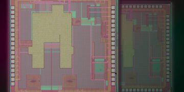


The process developed at KIT manages low temperatures and allows high resolution for applications in optics and semiconductor technology – Publications in Science. A process developed (3D printed glass without sintering) at the Karlsruhe Institute of Technology (KIT) creates nanoscale quartz glass structures that can be printed directly onto semiconductor chips.
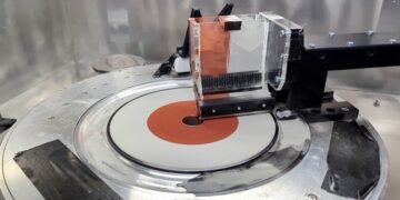
An organic-inorganic polymer resin hybrid serves as a starting material for 3D printing of silicon dioxide. Since the process does not require sintering, the required temperature is relatively low. At the same time, high resolution enables nanophotonics in visible light.
The research team reports in the journal Science. (DOI: 10.1126/science.abq3037)
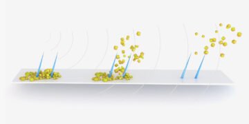
Quartz printing (3D Printed Glass without Sintering) glass based on pure silicon dioxide at the microscale and nanoscale opens up new opportunities for many applications in the fields of optics, photonics and semiconductor technology.
However, at the moment, methods based on traditional sintering dominate. The temperature required to ignite silicon dioxide nanoparticles is above 1,100 degrees Celsius, too hot for direct application to semiconductor chips.
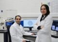
A research team of Dr. Jens Bauer from the KIT Institute of Nanotechnology (INT) has now developed a new method to produce transparent quartz glass with high resolution and good properties that work at low temperatures. Organic-inorganic hybrid polymer resin serves as the starting material
Bauer, who leads the Emmy Noether “Nanoarchitected Metamaterials” small research group at KIT, and colleagues at the University of California, Irvine and the medical technology company Edwards Lifesciences in Irvine presents the process in the journal Science.
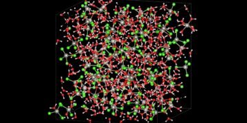
A well-developed organic-inorganic polymer resin hybrid serves as the starting material. The liquid resin is made of polyhedral oligomeric silsesquioxane (POSS) particles: small silicon dioxide molecules that contain organic functional groups.
Once the nanostructure is fully 3D printed, it is heated in air to 650 degrees Celsius. In this process, the organic matter is expelled and, at the same time, the inorganic POSS particles are combined, creating a continuous micro- or nanostructure of fused silica.
The temperature required is only half of the method based on sintering of nanoparticles. The construction is resistant to even harsh chemicals and temperatures
“The low temperature allows optical structures to be printed directly onto semiconductor chips with the resolution required for visible light nanophotonics,” says Bauer.
In addition to beautiful optics, the quartz glass thus produced has good functional properties and is easy to process.
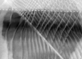
The Karlsruhe and Irvine team used POSS resin to print a variety of nanoscale structures, including photonic crystals with 97 nanometer free-standing beams, parabolic microlenses, and nanostructured multilens microlenses.
“Our process makes it possible to obtain structures that are resistant to harsh chemicals or temperatures,” explains Bauer.
“The INT team led by Jens Bauer is the best of the 3DMM2O cluster,” says Professor Oliver Kraft, vice president of research at KIT.
The research results published today in Science are just one example among many successes in promoting young talent within the cluster.
” The collaboration between KIT and the University of Heidelberg, is a combination of science from Nature and engineering have a strong curriculum.
Its aim is to take the 3D additive manufacturing process to the next level – from the molecular level to the macroscopic dimension.
Source: Karlsruhe Institute of Technology

