To tune the band gap, a key parameter in controlling the electrical conductivity and optical properties of semiconductors, researchers typically engineer alloys, a process in which two or more materials are combined to achieve properties that otherwise could not be achieved by a pristine material.
But engineering band gaps of conventional semiconductors via alloying has often been a guessing game, because scientists have not had a technique to directly “see” whether the alloy’s atoms are arranged in a specific pattern, or randomly dispersed.
Now, as reported in Physical Review Letters, a research team led by Alex Zettl and Marvin Cohen—senior faculty scientists in the Materials Sciences Division at the Department of Energy’s Lawrence Berkeley National Laboratory (Berkeley Lab), and professors of physics at UC Berkeley—has demonstrated a new technique that could engineer the band gap needed to improve the performance of semiconductors for next-generation electronics such as optoelectronics, thermoelectrics, and sensors.
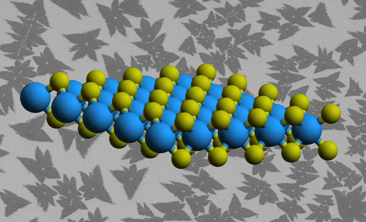
For the current study, the researchers examined monolayer and multilayer samples of a 2-D transition metal dichalcogenide (TMD) material made of the alloy rhenium niobium disulfide.
Electron microscopy experiments revealed meandering stripes formed by metal atoms of rhenium and niobium in the lattice structure of the 2-D TMD alloy.
A statistical analysis confirmed what the research team had suspected—that metal atoms in the 2-D TMD alloy prefer to be adjacent to the other metal atoms, “which is in stark contrast to the random structure of other TMD alloys of the same class,” said lead author Amin Azizi, a postdoctoral researcher in the Zettl lab at UC Berkeley.
Calculations performed at Berkeley Lab’s National Energy Research Scientific Computing Center (NERSC) by Mehmet Dogan, a postdoctoral researcher in the Cohen lab at UC Berkeley, demonstrated that such atomic ordering can modify the material’s band gap.
Optical spectroscopy measurements performed at Berkeley Lab’s Advanced Light Source revealed that the band gap of the 2-D TMD alloy can be additionally tuned by adjusting the number of layers in the material. Also, the band gap of the monolayer alloy is similar to that of silicon—which is “just right” for many electronic and optical applications, Azizi said. And the 2-D TMD alloy has the added benefits of being flexible and transparent.
The researchers next plan to explore the sensing and optoelectronic properties of new devices based on the 2-D TMD alloy.


