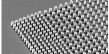


Good space. Hello metasurface! Said metasurfaces could help build thinner optical systems in the future, increasing functionality. The problem: Traditional manufacturing processes can often produce very small meta-surfaces, less than one millimeter square.
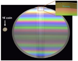
Fraunhofer IOF researchers have now succeeded for the first time in using electron beam lithography to create a metasurface with a diameter of almost 30 centimeters – a world record (Metasurfaces are thin rather than optically thick). The scientists have now published their method in the Journal of Micro/Nanopatterning, Materials, and Metrology.
In addition, the new metastructure will appear publicly for the first time from June 27 to 30 at the LASER World of Photonics in Munich. “After 500 years of my eyes and glasses, it’s time to think about the future,” said Dr. Falk Eilenberger, head of the department of micro and nanostructured optics at the Fraunhofer Institute for Optics applied to precision engineering IOF.
The so-called metasurfaces can be another thing here. These are the things that focus all their attention on working on the surface and understand this work on the surface thanks to nanostructures. Eilenberger describes the difference in classical space as follows: “In space, the function is defined by macroscopic geometry.
This is why space is so big and crooked. Now we have a meta interface instead. It’s thin and structured on a scale less than the wavelength of light.”
Metasurfaces have long been used in science and research. However, the equipment here usually measures only a few square millimeters. It is sufficient for academic research, but not for many industrial applications and certainly not a good choice for future classic space.
Therefore, researchers at the Fraunhofer IOF in Jena answered the question of how new metasurfaces can be obtained on a large scale. As a result, they show the first metasurface with a diameter of 30 centimeters.
“We are not the inventors of metasurfaces,” Eilenberger said. “But we just have to show it on a larger scale.”
High-resolution architecture has high accuracy and performance
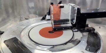
But how did the researchers arrive at this remarkable fact? Answer: With the help of electron beam lithography. “For the production of our metasurface, we use a special technique of electron beam lithography, called character projection,” said Prof. Dr. Uwe Zeitner, researcher at Fraunhofer IOF and member of the institute’s scientific management board explains.
A character map is a system that divides values into a number of units. An electron beam is used to create each of these sub-patterns in sequence. This makes it possible to create complex structures with high design and performance.
“With the help of character projection, very high-quality structures can be exposed simultaneously and at very high speed. This is unusual for electron lithography,” Zeitner continued. Together with his Fraunhofer colleagues, Dr. Michael Banasch and Dr. Marcus Trost explains Prof. Zeitner describes the potential of electron beam lithography for the fabrication of micro and nano optics on large surfaces in a paper currently published in the “Journal of Micro/Nanopatterning, Materials, and Metrology”.
Through their essay, the authors show that conventional lithographic techniques often reach their limits for producing large-scale structures. “Because of the small part of the structure under the long wavelength, high-resolution electron beam lithography is fundamentally well qualified for the production of metastructures,” explains the researcher.
“However, this technology is very slow, so far it has only been used for objects with small areas – mostly in the order of a few millimeters. At high altitudes, exposure times reach unreasonably fast values. “Using character projection, scientists can now address both the high resolution of electron beam lithography and the large surface area of the design without the exposure time ‘exploding’, according to Uwe Zeitner.
The authors of the article thus show that electronic lithography can be a technique for creating micro- and nano-optical structures on large surfaces.
Don’t downsize while increasing functionality at the same time
New manufacturing technologies could help build thinner optical systems in the future. “This technology can revolutionize optical imaging systems”, said Falk Eilenberger. “Because it makes it possible to reduce the size of the system while increasing the optical performance.
“Uwe Zeitner adds a quick example: “Such a large meta-surface is particularly useful for compact optics where a large switching area is required. Small apertures, for example synthetic/integrated mirrors the truth.
Even if the optics are small and popular, such a method can be used to obtain useful features. Other applications may include advanced spectroscopy or computer-generated holograms.
Source: Fraunhofer Institute for Applied Optics and Precision Engineering


