New promises of nanostructures for advanced electronics, Scientists at Tokyo Metropolitan University have produced various nanostructures of metal dichalcogenides that assemble into planes to form bonds,
They grew layers of molybdenum disulfide multilayer structures from the edges of niobium-doped molybdenum disulfide shards, creating a large, glued, planar heterostructure.
They showed that these materials can be used to make transistors (TFETs) to create new low power circuits.
Field effect transistors (FETs) are an integral part of almost all digital circuits. They control the flow of current through it based on the voltage across it.
Although metal oxide semiconductor FETs (or MOSFETs) are the majority of FETs in use today, research continues for the next generation to drive faster Desirable and compact with low power consumption.
This is where tunneling FETs (or TFETs) come in. TFET is based on the quantum tunneling effect, the effect of electrons being able to pass through a barrier that cannot be crossed due to the quantum effect.
Although TFETs use less power and have long been proposed as a promising alternative to traditional FETs, scientists have yet to find a way to implement the technology in a feasible manner.
A group of scientists from Tokyo Metropolitan University led by Associate Professor Yasumitsu Miyata is working on making nanostructures from transition metal dichalcogenides, a mixture of transition metals and group 16 elements.
Transition metal dichalcogenides (TMDCs, two chalcogen atoms for one metal atom) are attractive materials for TFET fabrication.
Their recent success has allowed them to assemble an unprecedented piece of TMDC crystal. Now they have turned their attention to the multilayer structure of TMDC.
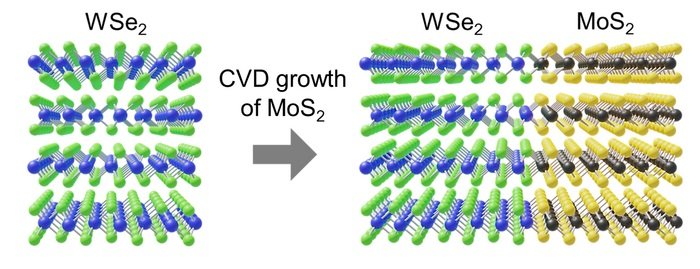
Using a chemical vapor deposition (CVD) method, they demonstrated that they could create a separate TMDC from the edge of a crystal plane assembled on a surface.
The result is an in-plane connection that spans multiple levels.
Most of the works on TMDC junctions use monolayers stacked on top of each other; In fact, despite the excellent constitution of the plane junction, previous efforts could not achieve the large gap of holes and electrons necessary to operate the TFET.
After demonstrating the strength of their method using molybdenum disulfide derived from tungsten diselenide, they turned to molybdenum disulfide doped with niobium, a p-type semiconductor.
By creating a multilayer structure of uncoated molybdenum disulfide, a semiconductor-like material, the team achieved a large p-n center TMDC with an unprecedented charge concentration.
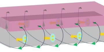
In addition, they found that the junction showed a tendency to negative differential resistance (NDR), where an increase in voltage leads to a small increase in current, the main part of tunneling and the first step necessary for nanomaterials to enter TFET.
The process of the working group is also able to move over a large area, making it suitable for implementation during circuit production. This is an exciting new development for modern electronics, hopefully it will find its way into future applications.
Source: Tokyo Metropolitan University


