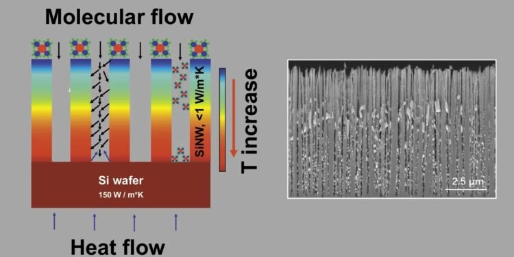
Nanoscale coatings with mechanical properties play an important role in many sensory, electronic and photo applications. An international research team – coordinated by Leibniz IPHT in Jena, Germany – succeeded for the first time in seeing the new growth effect of tin coating on a nanostructured silicon surface, Active Surface Refining.
Thanks to the knowledge gained, the chemical composition of the important materials applied can be controlled and analyzed in the future, opening new applications in the field of biophotonics, energy or transport. The results were published in the journal Small.
Layers with tin are required for a variety of electronics and materials in the electrical industry as well as sensor technology or photovoltaics. Researchers from the Leibniz Institute of Photonic Technology (Leibniz IPHT) studied the process of creating nanoscale tin layers with scientists from Germany, Russia and Britain and gathered their findings in the famous magazine Small.
The precursors for the observed growth process of thin films with tin are soft silicon-based materials in the form of nanowires with a diameter of less than 100 nanometers. In an experimental experiment, the researchers showed for the first time a distribution effect of tin on the side of these silicon nanostructures: layers with different oxidation states were placed along the entire length of the semiconductor nanowires by chemical deposition in a temperature of 600 degrees Celsius.
“By understanding how the tin coating grows and the factors that affect this growth process, we create the conditions to control the coating process precisely. This allows the tin to be properly refined and given the following properties required to work in the conditions specified earlier,” Dr. Vladimir Sivakov, head of the silicon nanostructures group at Leibniz IPHT says, who researched and discovered the growth with his team.
The use of tin cloth is important
Nanoscale coating with tin makes different optical and electrical properties possible, among other things, to improve the research and development of optical and biophotonic systems. A layer can be used as a UV-SERS-activated surface Raman scattering spectroscopy (SERS), which can be applied to determine the fingerprint of living cells using SERS-activated metal nanostructures. In addition, there are application areas in gas sensors where tin reacts with gas as a highly sensitive layer. Applications and high performance lithium-ion batteries for electromobility and thermal energy storage are possible, the tinned anodes provide high electronic conductivity.
Process and growth potential of tin layer
The researchers investigated the growth of pigment-based layers on nanostructured surfaces using optical and spectroscopic techniques. Unlike flat, unstructured silicon, in which deposition takes place individually, the surface of semiconductor nanowires is covered with tin-containing crystals of various sizes and shapes ‘the whole length.
The results presented in the paper show the formation of different tin oxide systems on the side of nanostructured silicon, which can be identified as tin dioxide (SnO2) in the upper part, tin monoxide (SnO) in the middle and metallic tin (Sn) in. part of the land.
The amount and distribution of Sn precipitates and its oxides SnO and SnO2 can be well defined by the length, diameter, porosity and spacing of silicon-based semiconductor nanostructures. In addition to these geometric parameters, the researchers can reveal the formation of products with hydrocarbons as reducing factors that reduce tin oxide as another factor affecting the distribution of tin layers formed.
The thermal conductivity of the silicon structure and how the temperature distribution around the nanowires during high temperature steam input can also affect the formation of different tin oxide systems.
Source: Leibniz Institute of Photonic Technology


