


Researchers successfully develop nanoLED systems, A new technique produces perovskite nanocrystals where they are needed, so solid materials can be incorporated into nanoscale devices.
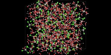
Halide perovskites are a family of materials that have attracted attention for their high optoelectronic properties and potential applications in devices such as high-performance solar cells, light-emitting diodes, and lasers.
These are widely produced in micrometer or thin film applications. The successful combination of these materials at the nanoscale can open up other remarkable applications, such as light sources, photodetectors and memristors. However, achieving this integration is still a challenge because this soft material can be damaged by manufacturing and processing.
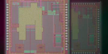
To overcome this problem, MIT researchers have developed a method that allows individual halide perovskite nanocrystals to grow when needed and controlled conditions, within 50 nanometers. (One piece of paper is 100,000 nanometers.) The size of the nanocrystals can also be controlled precisely using this method, which is important because the size affects their properties. Since this material is grown in an area with the desired characteristics, the lithographic process that can cause damage is unnecessary.
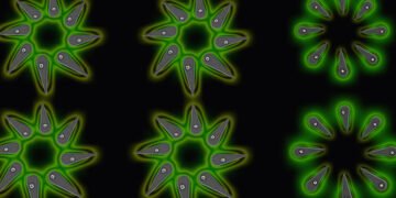
This process is also scalable, flexible, and compatible with traditional manufacturing processes, so it can enable nanocrystals to be incorporated into functional nanoscale devices. The researchers used it to make several nanoscale light-emitting diodes (nanoLEDs) – small crystals that emit light when activated by electricity. Such networks may have applications in optical communications and computers, gapless microscopes, new types of quantum light sources, and high-density, high-resolution displays for augmented and virtual reality.
“As our work shows, it is important to develop new design methods for integrating nanomaterials into functional nanodevices. Breaking the traditional boundaries of nanofabrication, materials engineering, and device design, these techniques can allow us to manipulate matter at the nanoscale, enabling us to realize device platforms that are not conventional technologies to meet the needs emerging technology, ”said Farnaz Niroui, EE. Landsman Career Development Assistant Professor of Electrical Engineering and Computer Science (EECS), member of the Research Laboratory of Electronics (RLE) and lead author of the new job description.
Niroui’s co-authors include author Patricia Jastrzebska-Perfect, an EECS graduate student; Weikun “Spencer” Zhu, a graduate of the Department of Chemical Engineering; Mayuran Saravanapavanantham, Sarah Spector, Roberto Brenes and Peter Satterthwaite, all EECS graduate students; Zheng Li, RLE postdoc; and Rajeev Ram, Professor of Electrical Engineering. The research is published today in Nature Communications.
Small crystal, big challenge
Incorporating halide perovskites into nanoscale on-chip devices is extremely challenging using nanoscale manufacturing techniques. In the same way, a thin film of bright perovskites can be created using the lithographic process, which requires a solvent that can damage the material. Alternatively, small crystals are first formed in the solution, then selected and placed in the solution at the desired values.
“In both cases, there is a lack of control, resolution and input power, which limits how the material can be expanded into nanodevices,” says Niroui.
Instead, he and his team developed a way to “grow” halide perovskite crystals in the exact spot on the desired surface to create a nanodevice.
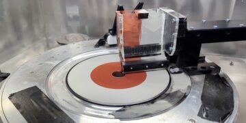
The main of their method is to find solutions used in the growth of nanocrystals. To do this, they create a nanoscale model in a small well that contains the chemical structure of the growing crystal. They change on the surface of the model and in the interior of the well, controlling the property known as “wettability” so that the solution containing the perovskite material does not collect on the surface of the model and is held in to do.
“Now you have these little things, the detectors can grow out of it,” he said.
And that is exactly what is happening. They put a solution containing halogenated perovskite to grow in the matrix, and as the solvent evaporates, the material grows and forms small crystals in each well.
Different and modular systems
The researchers found that the shape of the wells plays an important role in controlling the position of the nanocrystals. If a square well is used, due to the effect of nanoscale forces, the crystal has an equal chance of being placed in the four corners of the well. For some applications this may be sufficient, but for others it is important to be very precise in the placement of the nanocrystals.
By changing the shape of the well, the researchers were able to create these forces at the nanoscale so that the crystal could be placed precisely in the desired location.
As the solvent evaporates into the well, the nanocrystal experiences a pressure extension that creates a guiding force, and the specific direction is determined by using the asymmetric shape of the well.
“This allows us to be very precise, not only in the growth, but also in the concentration of these nanocrystals,” explains Niroui.
They also discovered that they could control the size of the crystals that formed in the well. Changing the size of the well to make the solution larger or smaller produces larger or smaller crystals.
They demonstrated the effectiveness of their method by creating a nanoLED system. In this process, each nanocrystal is converted into a nanopixel that emits light. These high-density nanoLED systems can be used for optical communication in on-chip computers, quantum light sources, microscopy, and advanced displays for embedded applications in virtual reality.
In the future, researchers want to explore other possible applications for these small lights. They also want to test the limits of these tiny devices and try to successfully integrate them into quantum systems. Away without fire continues nanometric together, the process is open to other opportunities to develop respective nanodins based on their halogium.
The process they give to researchers studying in the nanocrystal level, expectations, will inspire to teach others to study the following and other unique things. “Studying nanoscale objects by high-resolution methods often requires that the objects be precisely mapped to their structure on the scale,” Jastrzebska-Perfect adds. “By providing local control, our system can improve how researchers evaluate and optimize the properties of applications for different applications.”
“The team has developed a very clever method for the deterministic synthesis of individual perovskite nanocrystals and substrates. They can control the precise concentration of nanocrystals in an unprecedented scale, allowing for the creation of efficient nanoscale LEDs based on single nanocrystals,” Ali Javey, professor of electrical engineering and computer science at The University of California at Berkeley says. , who was not involved in this research. “This is an exciting project because it overcomes an important challenge in the field.”
Source: MIT


