


Moiré 2D materials without stacking, twisting
Cornell researchers have found a new way to make moiré patterns—tiny structures at the atomic level that can give materials special quantum properties—without using the tricky and hard-to-control method of stacking and twisting layers.
Since 2018, scientists have been really interested in moiré materials because when layers of materials like graphene are slightly twisted, they can show amazing properties like superconductivity.
Moiré patterns happen when thin layers of materials are stacked not perfectly aligned. This creates changes in the atomic structure that can change how electrons move through the material. These changes can lead to interesting quantum behaviors, including magnetic effects, insulating states, and superconductivity.
But making these moiré patterns has usually meant manually twisting and stacking 2D materials, which isn’t very reliable or easy to scale up.
Now, a new method for making moiré patterns has been developed.
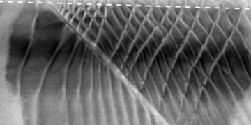
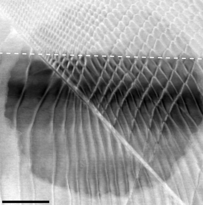
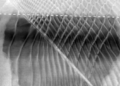
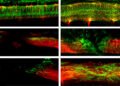
This method, published on May 27 in the Proceedings of the National Academy of Sciences, uses thin films to apply controlled strain to layers of molybdenum disulfide. This creates moiré superlattices across the material. This approach offers a more predictable and scalable way to make quantum materials using standard manufacturing techniques.
“Strain engineering is already a common part of semiconductor manufacturing,” said Judy Cha, the Rick and Betty Tsai Ph.D. 1981 Professor in Materials Science and Engineering at Cornell.
“For many years, companies have used methods like silicon-germanium alloys and stressed metal coatings to deliberately strain silicon and improve transistor performance.”
Cha was inspired to use this technique after seeing that metal stressor films could strain 2D materials.
She realized this method could create moiré patterns because the top layers of the material would stretch or compress differently than the layers below.
To create this strain, the researchers placed patterned stressor films on molybdenum disulfide flakes.
These films stretched and compressed the top layers, creating different strain areas across the material. Near the edges of the films, the strain was mostly biaxial, while further away, it was primarily uniaxial, leading to different moiré shapes.
The different strain areas caused localized electric polarization in molybdenum disulfide, a material that usually doesn’t have this property.
At the boundaries between moiré areas, small shifts in the atomic structure created in-plane polarization patterns whose direction depended on the strain shape.
The researchers are now looking into using these polar areas in working electronic devices.
“Since the polarization can be switched with an electric field, this effect could potentially be used to change electrical resistance at the nanoscale,” said Cha, who also leads the Cornell NanoScale Facility.
“This could make it easier for researchers to study moiré physics.”
“This is a standard lithography process that everyone who makes devices does every day,” Cha added.
“I hope this opens the door for people who haven’t done a lot of layer stacking to explore this method.”
Source: Cornell University


