


Smallest Semiconducting Nanotubes
Scientists in Japan have made some of the smallest semiconducting nanotubes ever created. These nanotubes are made from a material called molybdenum disulfide and are just 1 nanometer wide. To make them, University of Tokyo researchers used a special method where they grew the material inside tubes made from boron nitride. This helped them create very uniform nanotubes that are stable at such a tiny size. These nanotubes are much thinner than a human hair—about 100,000 times thinner.
This research supports old theories about how ultrafine materials behave and may help develop smaller electronics.
A few years ago, carbon nanotubes were the big focus in nanotechnology, but now there’s a new option. Molybdenum disulfide nanotubes could offer better performance in electronic devices, high-precision sensors, and studies of quantum physics. Though still in the experimental stage, they show promise for future technologies.
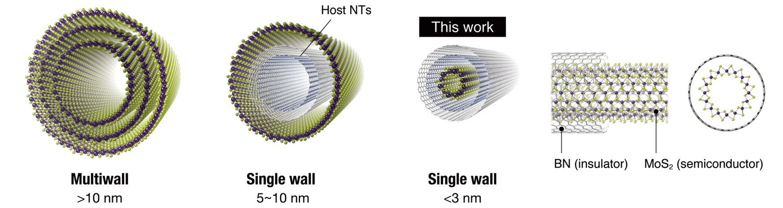
“We made the synthesis of semiconducting nanotubes with precise atomic structure and very small diameters. The design, where a semiconducting MoS2 nanotube is wrapped around an insulating boron nitride (BN) nanotube, is useful for gate-all-around transistors, which are among the most advanced types of transistors,” said Associate Professor Yusuke Nakanishi from the Department of Advanced Materials Science at the University of Tokyo.
“Our research shows how we can control the structure of inorganic semiconducting nanotubes at the atomic level. We also showed, through experiments, that the bandgap—something that determines how a material behaves as a semiconductor—gets smaller as the nanotube diameter decreases, which matches predictions made over 25 years ago.”
Traditional methods for creating nanotubes usually result in larger diameters, multiple layers of tubes, and structures that are not well-controlled or irregular.
Nakanishi and his team created nanotubes that are just 1 nanometer wide, with clearly defined atomic structures. They did this by using chemical reactions inside the narrow space of BN nanotubes.
This confined space helps control the formation of MoS2 nanotubes, which are otherwise hard to make, and leads to well-organized atomic arrangements, which are important for use in engineered devices.
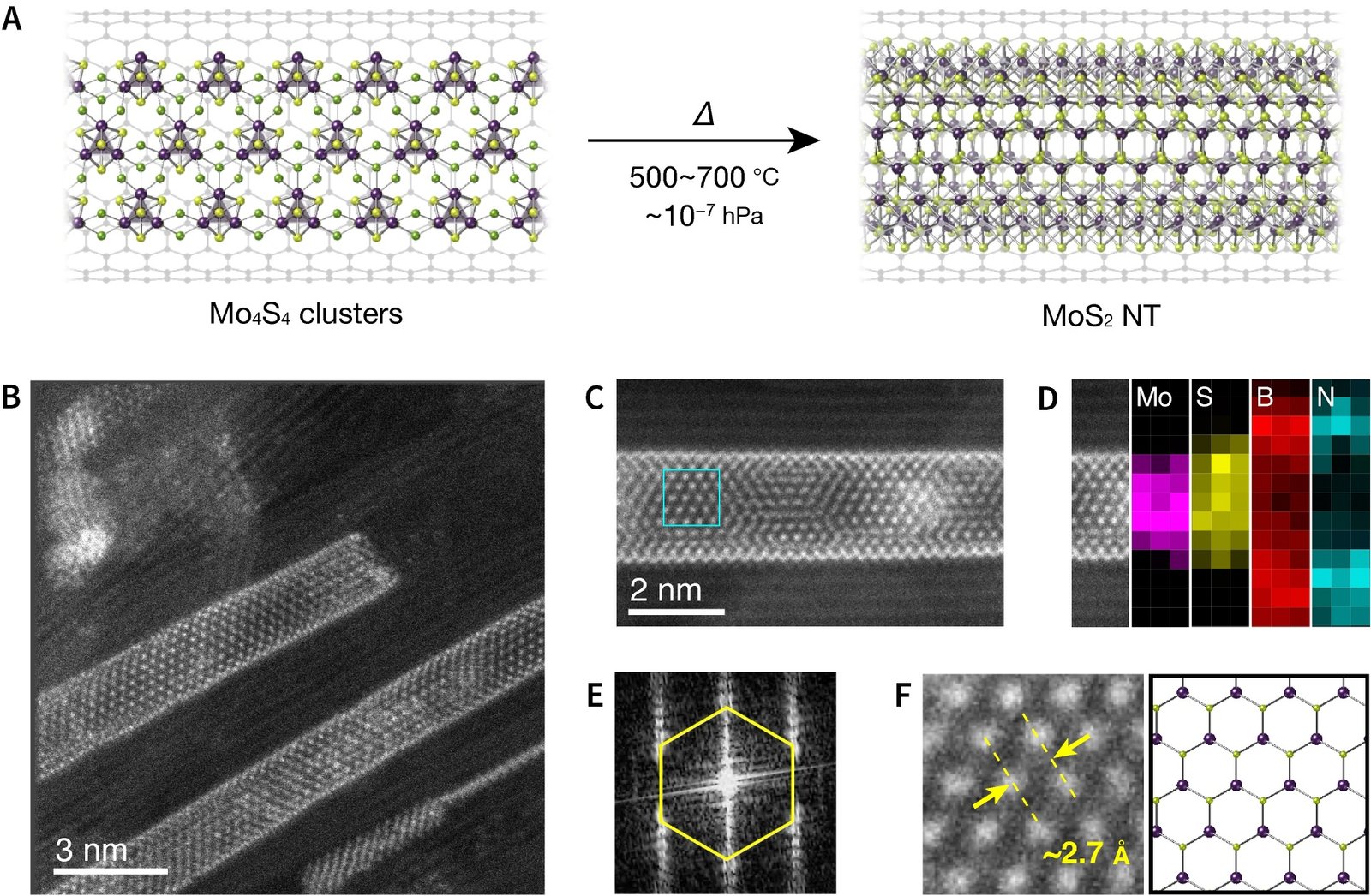
In nanotubes, even small changes in structure can greatly influence their properties. If the structure can be carefully controlled, the properties become more uniform, which is important for making transistors that work reliably and consistently. “Their main benefit is the ability to control the structure at the atomic level,” said Nakanishi.
“Right now, silicon transistors are made by cutting into bulk silicon, but as they get smaller, it’s harder to keep the structure perfect, and defects can have a big effect. Carbon nanotubes also face challenges for use in transistors, because even tiny differences in structure can change how they behave, including whether they act like metals or semiconductors.
Our nanotubes could provide a more dependable way to create very small semiconductor channels with consistent properties,” he added. However, practical uses are probably still a few years away, and there are still major challenges before working transistor devices can be made.
The team wants to increase the length of the nanotubes from the current limit of a few hundred nanometers to about 1 micrometer, which is 1,000 nanometers or one-thousandth of a millimeter.
Another future goal involves materials: the method could also be used to make other types of inorganic nanotubes, including those with magnetic or superconducting properties.
The researchers hope this work will help expand nanotube research beyond carbon-based systems and open up new possibilities for a wider range of atomically precise nanotube materials used in research, sensing, and smaller, faster devices.
Source: University of Tokyo


